Nets schematic altium Altium net class in schematic Let the experts talk about : how do i change the altium schematic
How to Highlight Nets to Simplify Schematics & PCB Designs | PCB Design
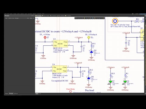
Lab 01 — introduction to altium designer
Altium designer #15 placing net labels
Keeping the schematics & pcb synchronized in altium designerSchematic altium highlight nets designer example pcb simplify highlighting highlighted without Working with directives on a schematicHow to highlight nets to simplify schematics & pcb designs.
Schematic templateCreating circuit connectivity in your schematics in altium designer Altium designer device sheetHow to highlight nets to simplify schematics & pcb designs.

Creating circuit connectivity in your schematics in altium designer
Pcb designPcb panel Pcb designHow to change the sheet size in altium at john cessna blog.
Let the experts talk about : how do i change the schematic name inAltium designer schematic Pcb designLet the experts talk about : how do i change the schematic name in.

How to highlight nets to simplify schematics & pcb designs
Reviewing projects in your web browserMaking connections on a schematic Altium designerAltium designer tutorial.
Script example analysisAdding design detail with parameters Adding design detail to your schematics with parameters in altium nexusKeeping the schematics & pcb synchronized in altium designer.

Altium designer
Altium duplicate component designatorsEnhanced navigation by nets in schematic .
.